TSMC CEO outlines efforts to enhance cost-effectiveness of High-NA EUV
TSMC's CEO is addressing the cost challenges associated with High-NA EUV lithography adoption, signaling the company's cautious approach to implementing next-generation semiconductor manufacturing technology. The effort reflects broader industry tensions between technological advancement and economic viability in advanced chip production.
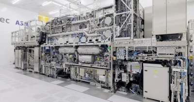
TSMC's focus on cost-effectiveness for High-NA EUV represents a critical inflection point in semiconductor manufacturing evolution. High-NA EUV (Extreme Ultraviolet) lithography represents the next frontier in chip density and performance, but requires substantial capital investment and operational expertise. The company's emphasis on enhancing cost-effectiveness rather than rushing deployment suggests realistic assessment of economic constraints in the industry.
The semiconductor industry faces intensifying pressure to maintain Moore's Law progression while managing exponential increases in fabrication complexity and costs. TSMC's cautious approach follows broader trends where leading foundries balance innovation speed against profitability. As manufacturing nodes shrink below 3nm, each successive generation demands disproportionate R&D spending and equipment investment, making financial prudence essential for long-term viability.
For the broader ecosystem, TSMC's deliberate High-NA EUV strategy has cascading implications. Chip designers, including AI accelerator manufacturers and cryptocurrency hardware producers, depend on advanced nodes for competitive advantage. Delays or measured adoption timelines could affect product roadmaps across industries reliant on cutting-edge silicon. The approach also signals that technological leadership requires financial discipline—companies cannot simply adopt new processes; they must optimize implementation economics.
Investors should monitor TSMC's capital expenditure guidance and High-NA EUV timeline announcements. Success in cost optimization could accelerate adoption across the industry, while continued challenges might sustain current manufacturing constraints. The company's execution on this challenge directly influences semiconductor supply dynamics and competitive positioning in AI and advanced computing markets.
- →TSMC prioritizes cost optimization over rapid High-NA EUV adoption, reflecting economic realities of advanced semiconductor manufacturing
- →High-NA EUV represents necessary but expensive next-generation technology requiring substantial capital and operational investment
- →Manufacturing delays or measured rollout could impact AI accelerator and advanced chip availability across industries
- →TSMC's approach emphasizes financial discipline in technology transitions, balancing innovation with profitability constraints
- →Industry-wide High-NA EUV adoption timeline depends on successful cost-effectiveness improvements from leading foundries